
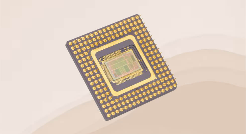
We already covered the main ideas behind Real Mode & Protected Mode in one of our previous posts. This article will build on those concepts and take a deeper look at the history and evolution of the x86 family of CPUs. But rather than simply looking at the innovations introduced with each new chip, we need to understand how the architecture accumulated over time, from its origins in the early 70s up until the launch of the 486.
Every time a new student starts learning x86 assembler with us, it's not rare to hear them complain that many aspects of the instruction set look arbitrary. An accumulator that some instructions insist on, a base register that is the only one allowed to point at memory, a parity flag nobody seems to use, and an addressing scheme that adds two 16-bit numbers together in a very strange way.
The majority of teaching resources out there will help you write your first lines of x86 code, assemble it, link it, and as proceed as soon as the output matches what you were expecting. I try to always explain the evolution of the x86 family of CPUs, so every aspect of our code makes a little bit more sense.
None of these things are arbitrary, of course. Each one is a decision someone made under pressure, usually to keep old software running on a new chip. If you want to really understand x86 (and especially if you want to program a 486 under DOS), the best place to start is not the 486 manual. It's the story.
Here is the family tree we're going to walk through:
| Year | Chip | Width | Addr. space | What it added that still shows up in x86 |
|---|---|---|---|---|
| 1971 | 4004 | 4-bit | 4 KB prog. ROM | Intel's first CPU, for a Busicom calculator |
| 1972 | 8008 | 8-bit | 16 KB | Register set A, B, C, D, E, H, L; little-endian order and a parity flag, both inherited from the Datapoint 2200 terminal it was designed for |
| 1974 | 8080 | 8-bit | 64 KB | 16-bit register pairs (BC, DE, HL), a real stack pointer, a separate 256-port I/O space with IN/OUT |
| 1976 | 8085 | 8-bit | 64 KB | One 5 V supply; address and data multiplexed on the same pins to save pins |
| 1978 | 8086 | 16-bit | 1 MB | Segmentation, a prefetch queue, 16-bit registers that contain the 8080's 8-bit ones |
| 1979 | 8088 | 16-bit inside, 8-bit bus | 1 MB | The cheaper version IBM chose for the 1981 PC |
| 1982 | 80286 | 16-bit | 16 MB | Protected mode with segment descriptors and privilege rings |
| 1985 | 80386 | 32-bit | 4 GB | 32-bit registers, paging, virtual 8086 mode |
| 1989 | 80486 | 32-bit | 4 GB | On-chip cache and FPU, a 5-stage pipeline |
A table like this makes the evolution look neat and planned. It wasn't. Between these rows there are cancelled projects, a customer who walked away from its own chip, a stopgap that was supposed to last a couple of years, a sales campaign, a keyboard controller wired into the address bus, and a lawsuit.
Let's travel back to 1969 and see how it all happened!
A Calculator Chip: The 4004
The story starts with a Japanese calculator company. In 1969, Busicom asked Intel (then a young memory company) to build a set of custom chips for a new printing calculator. Instead of designing many single-purpose chips, Intel's team proposed something more general: a small programmable processor that would run the calculator's logic from ROM.
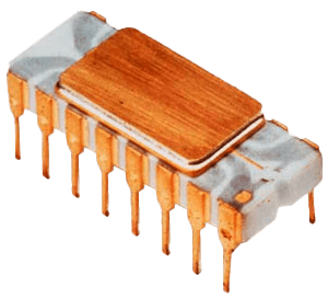
The result was the 4004, released on November 15, 1971, and designed by Federico Faggin, Ted Hoff, Stanley Mazor, and Masatoshi Shima. It had 2,300 transistors, ran at about 740 kHz, and could address 4 KB of program ROM.

The most important line in the 4004's story is not technical, though. Busicom had paid for the design and owned the rights. When Busicom ran into financial trouble in 1971, Faggin convinced Intel's CEO Bob Noyce to lower the chip's price in exchange for Intel getting out of the exclusivity deal. Intel paid back Busicom's $60,000 development costs and won the right to sell the chip to anyone (outside the calculator market).
That deal is why "a microprocessor" became something Intel could sell, rather than a part buried inside one calculator.
The Terminal That Didn't Want Its CPU: The 8008
At almost the same time, a second customer walked through Intel's door. In late 1969, Computer Terminal Corporation (CTC, later called Datapoint) asked Intel to build a chip for a programmable terminal called the Datapoint 2200.
This detail matters a lot: Intel did not design the instruction set of this chip. CTC's engineers Victor Poor and Harry Pyle did. They had already built the Datapoint 2200's processor out of dozens of discrete TTL chips, and they wanted Intel to squeeze that same design onto one piece of silicon.
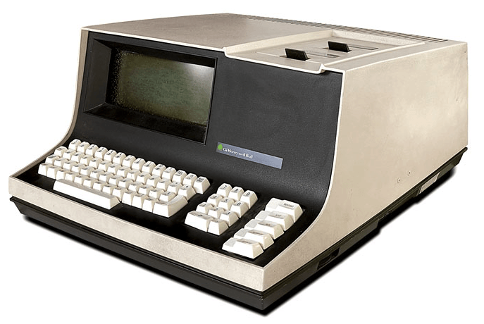
Intel was slow. Texas Instruments also tried to build the chip, but its samples were buggy and rejected. Meanwhile, CTC shipped the Datapoint 2200 in 1970 with its TTL processor anyway, and later moved on to a faster design. In the end, CTC voted to walk away from the project and leave the design to Intel instead of paying the $50,000 contract. Intel renamed it the 8008 and released it in April 1972 with 3,500 transistors and 16 KB of addressable memory.
So the ancestor of every x86 chip was designed by a terminal company, for a terminal, and then rejected by that terminal company. And two of the terminal's habits are still inside your PC today.
Why x86 is Little-Endian
The Datapoint 2200 processed numbers one bit at a time (a bit-serial design). If you're adding two numbers one bit at a time, you want to start with the lowest bit, because that's where the carry starts. So it made sense to store the lowest byte first in memory.
The 8008 copied the Datapoint's design, the 8080 kept compatibility with the 8008, and the 8086 kept compatibility with the 8080. Stephen Morse, the architect of the 8086, put it this way in his history of the early Intel processors:
"This inverted storage, which was to haunt all processors evolved from the 8008, was a result of compatibility with the Datapoint bit-serial processor."
That's why, on your 486 (and even in a more modern Core i9), this instruction:
mov DWORD ptr [buffer], 12345678h...stores the bytes 78 56 34 12 in memory.
Why x86 Has a Parity Flag
The second habit is the parity flag (PF), which tells you if the result of the last operation had an even number of 1 bits. It's one of those flags that beginners look at and wonder who on earth needs it.
The answer is: a terminal does! Morse again: "This permits testing for transmission errors, an obviously useful function for a CRT terminal." Data arriving over a serial line often carried a parity bit, and the Datapoint needed a fast way to check it.
Fifty years later, PF is still bit 2 of the x86 FLAGS register.
The 8080 and the Birth of the PC Hobby
The 8008 was slow and awkward, so Intel designed a much better successor. The 8080 was released in April 1974, with Federico Faggin as its primary architect and Masatoshi Shima on the detailed design. It had about 4,500 transistors, ran at 2 MHz, and could address 64 KB of memory.
The 8080 was not binary compatible with the 8008, but it kept the same register set and the same "flavor." More importantly, it added several things you will recognize as an x86 programmer:
- Register pairs: B and C could be used together as the 16-bit pair BC, and the same for DE and HL
- The HL pair as the main way to point at memory (
MOV A, Mreads the byte at address HL) - A real 16-bit stack pointer
- A separate I/O space with 256 ports, accessed with
INandOUT
That separate I/O space is the reason why, many years later, VGA registers live at "port 3C8h" instead of at a memory address.
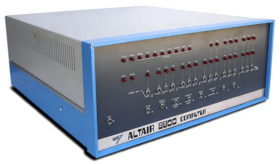
The 8080 powered the Altair 8800 and became the standard CPU for CP/M, the most popular operating system for small business computers in the late 70s. Suddenly, there was a lot of 8080 software out there.
And then Intel got some serious competition. Faggin and Shima left Intel and went to Zilog, where they built the Z80: a chip that could run 8080 machine code, but was faster, cheaper to build a computer around, and had more instructions. The Z80 started eating Intel's market.
The 8085: A Quiet Hint of What Was Coming
Intel's answer was the 8085, released in March 1976. The "5" in the name refers to its biggest selling point: it needed a single +5 V power supply, while the 8080 needed +5 V, -5 V, and +12 V.
To fit everything into a 40-pin package, the 8085 also multiplexed its bus: the same eight pins carried the low byte of the address first, and then the data. Remember this trick, because the 8086 uses it too.
There's a lovely footnote here: the 8085 had 12 new instructions, but Intel made a last-minute decision to document only 2 of them. The reason? To keep things simple for the next chip, which was already being designed. That chip was the 8086.
The Stopgap That Took Over the World: The 8086
In the mid 70s, Intel's big bet for the future was not the 8086. It was the iAPX 432, a very ambitious processor designed with object-oriented programming and high-level languages in mind. The 432 was late, and with the Z80 taking customers away, Intel needed something to sell in the meantime.
So, in May 1976, Intel started the 8086 project as a temporary product. Stephen Morse was the principal architect, Jim McKevitt and John Bayliss were the lead hardware engineers, and Bill Pohlman managed the project. The 8086 was released on June 8, 1978.
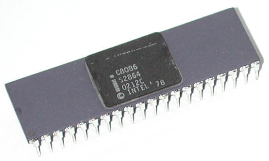
The brief was clear: the new chip had to address more than 64 KB, do 16-bit arithmetic, and (this is the important part) make it easy for existing 8080 software to move over.
Source Compatibility, Not Binary Compatibility
The 8086 cannot run 8080 machine code. Instead, Intel aimed for source compatibility: you could take your 8080 assembly program and translate it, line by line, into 8086 assembly. Intel even shipped a translator called CONV86 (available from 1978) to do this automatically. Morse described the goal like this: "the 8080 register set and instruction set appear as logical subsets of the 8086 registers and instructions."
For that translation to work, every 8080 register needed an obvious home in the 8086. And this is where the 8086's register names come from:
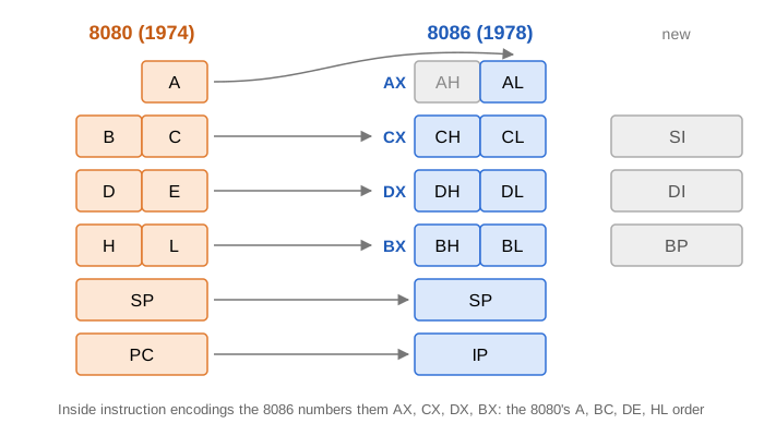
Here's a tiny 8080 routine and its 8086 translation side by side:
; 8080                     ; 8086
LXI  H, buffer             mov  bx, offset buffer   ; HL becomes BX
MOV  A, M                  mov  al, [bx]            ; A becomes AL
INX  H                     inc  bx
ADD  M                     add  al, [bx]
Now some of the "weird" things about x86 suddenly make sense:
- AX is the accumulator because 8080's A became AL. That's why
MUL,DIV,IN, andOUTinsist on using it, and why many instructions have shorter encodings when they use AL/AX. - BX is the base register because the 8080's memory pointer HL became BX. That's why, in 16-bit code, BX is the only one of AX, BX, CX, DX that can point at memory.
- CX is the count register (used by
LOOP,REP, and shifts) and DX is the data register (used for I/O port numbers and the high half of 32-bit results). - The 8080's flags byte became the low byte of the 8086's FLAGS register, and the instructions
LAHFandSAHFexist just to move that 8080-shaped byte in and out of AH.
Have you ever wondered why the 8086 numbers its registers in the order AX, CX, DX, BX (0, 1, 2, 3) inside instruction encodings, instead of the obvious A, B, C, D? It follows the 8080's order of register pairs: BC, DE, HL. Once A is placed first, BC becomes CX, DE becomes DX, and HL becomes BX.
And what does the "X" mean? According to Morse himself, nothing special. It was simply an arbitrary letter combining the "H" and "L" halves into one 16-bit register (as told to Vladimir Keleshev).
Segmentation: Reaching 1 MB with 16-bit Registers
The second big requirement was memory. Intel wanted 1 MB of address space, and that needs 20 address bits. But the 8086's registers were only 16 bits wide.
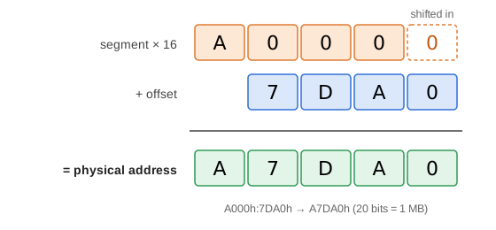
Morse's solution was segmentation. The chip has four segment registers (CS, DS, SS, and ES), and every memory access combines a segment with a 16-bit offset:
$$ \text{address} = \text{segment} \times 16 + \text{offset} $$
Multiplying by 16 is just a shift of 4 bits to the left. For example, if we want to write to pixel (160, 100) in VGA mode 13h, which lives at segment A000h:
mov  ax, 0A000h
mov  es, ax                       ; segment = A000h
mov  di, 320*100 + 160            ; offset  = 7DA0h
mov  byte ptr es:[di], 15         ; physical address = A0000h + 7DA0h = A7DA0h
Why 16 and not something bigger, like 256? Morse explained that with 8 bits of shift, "segments would be forced to start on 256-byte boundaries, resulting in excessive memory fragmentation."
Segmentation was cheap (a small adder in the chip) and it worked very well with the source-compatibility goal: an 8080 program expected a 64 KB world, so you could give it one segment and it would run unchanged, wherever in memory that segment happened to be.
But it also created a rule that haunted every DOS programmer for the next 15 years:
That rule is why C compilers for DOS had near, far, and huge pointers, and memory models with names like tiny, small, compact, and large. It's also why mode 13h is so beloved: 320 × 200 = 64,000 bytes, which fits in one segment!
Operation Crush and the 8088
The 8086 was not an instant hit. Motorola's 68000 and Zilog's Z8000 were more elegant 16-bit designs, and many engineers preferred them.
Intel's response was a sales campaign called Operation Crush, launched in a meeting in December 1979. Instead of selling the 8086 on raw specs, Intel sold it as a complete solution: development tools, support chips, documentation, and support. The goal was 2,000 "design wins" (products using the chip) in one year. They got nearly 2,500.
One of them was a small project inside IBM in Boca Raton.
A year after the 8086, Intel had released the 8088 (June 1, 1979). Internally it's the same 16-bit processor, but with an 8-bit external data bus. Every 16-bit memory access takes two bus cycles, so it's slower. But an 8-bit bus meant you could build the computer with cheap, plentiful support chips designed for the 8085. Intel also offered IBM a better price and could supply more units.
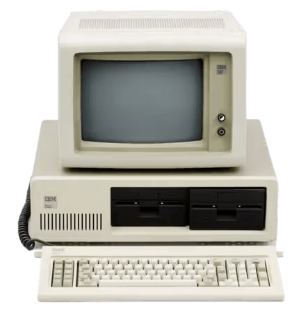
The IBM PC was launched on August 12, 1981, with an 8088 running at 4.77 MHz. That odd number comes from television: the PC used a 14.31818 MHz crystal (four times the NTSC color carrier, which the CGA video card needed), divided by 3.
IBM made one more decision that shaped the whole industry: it required a second source for the CPU, so it would never depend on a single supplier. That led to a 10-year technology exchange agreement between Intel and AMD, first signed in October 1981 and formally executed in February 1982. Keep that agreement in mind, because it comes back with the 386.
The famous "640 KB limit" is not a limit of the CPU. The 8088 could address 1 MB. It was IBM who placed video memory at address A0000h (that's 640 KB) and the BIOS ROM at the top of memory, leaving 640 KB of conventional memory for DOS and its programs.
The "temporary" 8086 family was now inside the machine that would define personal computing. From this point on, every new Intel chip had to run software written for the IBM PC. Compatibility was no longer a nice-to-have.
The 286: Protection Nobody Could Use
The 80286 was released on February 1, 1982, with 134,000 transistors. IBM used it in the PC/AT in 1984, running at 6 MHz.
The 286 was designed for multitasking operating systems. Its new protected mode changed what a segment register means: instead of holding a paragraph number, it holds a selector, an index into a table of descriptors. Each descriptor says where a segment starts (anywhere in 16 MB of memory), how big it is, and who is allowed to use it. The chip checks every memory access against those rules, and runs code in one of four privilege "rings."
On paper, this was fantastic. In practice, it had three problems:
- Segments were still limited to 64 KB.
- DOS programs routinely did arithmetic on segment values (adding 1 to a segment means "16 bytes further"). In protected mode, that produces a random selector and a crash.
- And the biggest one: once you switched to protected mode, you couldn't switch back.
Entering protected mode was as simple as setting one bit:
smsw ax          ; read the Machine Status Word
or   ax, 1       ; set the PE (Protection Enable) bit
lmsw ax          ; ...and there's no instruction to undo this
But DOS and the BIOS only worked in real mode. So how did the PC/AT get back? IBM built a hack into the motherboard: the program wrote a "shutdown code" into the CMOS memory, then asked the keyboard controller to pulse the CPU's reset line. The CPU rebooted, the BIOS noticed the shutdown code, and jumped back into the program, now in real mode. It worked, but it was painfully slow.
Bill Gates famously called the 286 "brain-damaged," mainly because it couldn't run several DOS programs side by side under a protected-mode operating system. Most 286 machines spent their lives running DOS in real mode, as a very fast 8086.
The A20 Gate
The 286 created another, stranger problem. On the 8086, the highest address you can form is FFFF:FFFF, which is 10FFEFh. That needs 21 bits, but the 8086 only has 20 address lines, so the top bit is lost and the address wraps around to the bottom of memory.
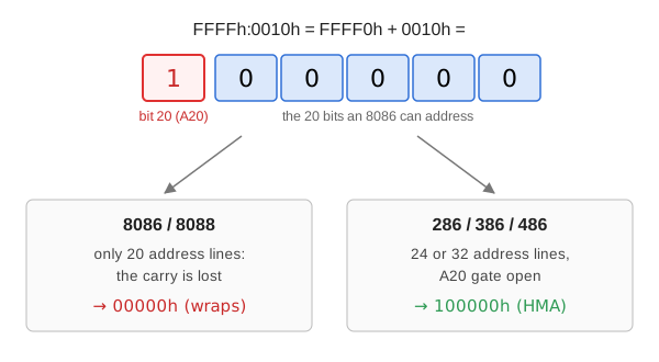
Some software depended on that wraparound. DOS's CP/M-style CALL 5 entry point relied on it to reach code at physical address C0h, and programs built with IBM/Microsoft Pascal used it as a space-saving trick. The 286 has 24 address lines, so it does not wrap, and those programs broke.
IBM's fix was to put a logic gate on address line 20 (A20), controlled by... a spare pin on the 8042 keyboard controller. With the gate closed, the PC/AT wraps at 1 MB like an 8086. With it open, real-mode code can reach the High Memory Area: 65,520 bytes just above 1 MB, which is where DOS=HIGH loads DOS.
This hack lived much longer than anyone expected:
A20M# pin to the CPU itself, and according to Intel's manuals, Intel only stopped supporting the A20 gate with the Haswell processors (2013). Source.
The 286 also had an undocumented instruction called LOADALL that could load the CPU's hidden segment caches directly, which tools like HIMEM.SYS used to reach extended memory without the slow reset trip. Hidden segment caches will come back very soon.
The 386: Intel Goes Alone
The 80386 was introduced as samples in October 1985, with mass production starting in June 1986. It had 275,000 transistors, and its chief architect was John Crawford (Pat Gelsinger, years later Intel's CEO, also worked on the project).
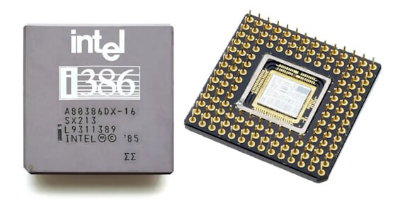
The 386 fixed the 286's problems one by one:
- 32-bit registers: EAX, EBX, ECX... (the "E" means extended), with AX and AL still living inside them.
- 4 GB segments: set every segment to start at 0 with a 4 GB limit and segmentation effectively disappears. This "flat model" is what DOS extenders like DOS/4GW (used by Doom) gave to C programmers.
- Paging: memory split into 4 KB pages with a two-level page table, which made real virtual memory possible.
- Virtual 8086 mode: a protected-mode task that behaves like an 8086. This is how EMM386 and Windows ran DOS programs safely, each believing it owned the machine.
- A way back: clearing the PE bit in CR0 returns to real mode. No keyboard controller needed!
mov  eax, cr0
and  al, 0FEh    ; clear PE
mov  cr0, eax    ; back in real mode, no reset required
Combining the way back with those hidden segment caches gave demo coders a favorite trick: unreal mode. You enter protected mode, load a segment register with a 4 GB limit, and return to real mode without reloading it. The CPU keeps using the cached 4 GB limit, so your real-mode program (with DOS still working!) can read and write all of memory using 32-bit offsets.
How did 32 bits fit into an instruction set designed for 16? Intel didn't add new opcodes for 32-bit operations. Instead, it added a bit to each code segment that sets the default size, plus two prefix bytes (66h for operand size and 67h for address size) that flip it for a single instruction. That's why a DOS program running in real mode on a 386 can still use EAX: the assembler simply adds a 66h prefix in front of the instruction.
The Business Decision
The 386's biggest story was not technical. Intel decided that the 386 would be single-source. As early as 1984, Intel had decided to stop cooperating with AMD, and it delayed and eventually refused to hand over the 386's technical details. AMD invoked arbitration in 1987, Intel cancelled the 1982 agreement, and the fight went on for years. AMD released its own Am386 in March 1991 (and sold one million of them by October of that year), and in 1994 the Supreme Court of California sided with AMD.
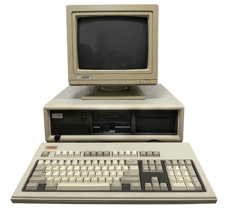
Then something happened that would have been unthinkable a few years before: IBM was not first. The Compaq Deskpro 386 shipped in September 1986, the first time a fundamental part of the IBM PC standard was moved forward by a company other than IBM.
And one more fun detail: some early 386 chips had a bug in 32-bit multiplication. Intel marked the affected chips with "16 BIT S/W ONLY", which was fine at the time because almost all software was still 16-bit anyway!
The 486: Same Instructions, New Engine
The 486 was announced at Spring Comdex on April 10, 1989, and it was the first x86 chip with more than one million transistors (about 1.2 million).
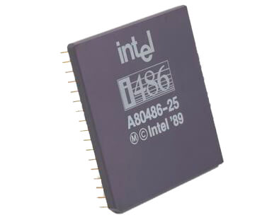
Here's the interesting part: the 486 added almost nothing to the architecture. A few instructions, like BSWAP, XADD, and CMPXCHG, and some control bits. What changed was the engine underneath:
- An 8 KB on-chip cache (16 KB on the later DX4)
- The floating-point unit integrated on the same chip
- A tightly pipelined five-stage design, where simple instructions finally finished in a single clock
Intel kept spinning variants: the 486SX (September 1991) with the FPU disabled, the clock-doubled DX2 (March 1992) that ran the core twice as fast as the motherboard, and the clock-tripled DX4 (March 1994).
For assembly programmers, the pipeline changed the rules of optimization. On the 8086, every instruction ran through microcode, and the "clever" complex instructions were often the fastest way to do things. On the 486, simple instructions became fast, and the old clever ones became the slow ones. The classic example is LOOP:
| Code | 8086 (clocks) | 486 (clocks) |
|---|---|---|
loop label (taken) | 17 | 7 |
dec cx + jnz label (taken) | 2 + 16 = 18 | 1 + 3 = 4 |
On an 8086, LOOP was the fast way to write a loop. On a 486, it's almost twice as slow as the "naive" version. If you read Michael Abrash's Graphics Programming Black Book, you'll see this shift everywhere: forget the microcoded tricks, use simple instructions, and keep your data inside the cache.
And Then It Got a Name
So why isn't the next chip called the 586? Because in 1991 Intel lost a trademark dispute over the name "386," when a judge ruled that a number was generic and could not be trademarked. AMD could call its chips "386" and "486" too.
Intel hired a branding agency and came up with a name instead of a number. The Pentium (from the Greek word for "five") was introduced on March 22, 1993. A few years later it would get those famous "with MMX technology" stickers, but that's another story.
Conclusion
Hopefully, by now, you can look at an x86 instruction set reference and see it as a geological record. Every layer was laid down by a specific event:
| The quirk | Where it came from |
|---|---|
| Little-endian byte order | The bit-serial Datapoint 2200 terminal (1970) |
| The parity flag | Checking transmission errors on a CRT terminal |
| AX as the accumulator, BX as the only memory pointer of the four | The 8080's A and HL, mapped for source compatibility (1978) |
IN/OUT and a separate port space | The 8080 (1974) |
| Segment:offset addresses and the 64 KB limit | Reaching 1 MB cheaply with 16-bit registers (1978) |
| The 640 KB limit | IBM's memory map for the PC (1981) |
| The A20 gate | Keeping wraparound-dependent DOS software alive on the PC/AT (1984) |
| Starting every PC in real mode | Every chip since the 8086 must boot like an 8086 |
The pattern is always the same. A chip is designed quickly, often as a stopgap, with one very practical goal in mind. Software starts to depend on its exact behavior (including its accidents). And from that moment on, every future chip has to carry that behavior forward, emulate it, or work around it with a hack.
That's the real lesson of x86 history: the architecture wasn't designed, it accumulated. And once you know the story, the quirks stop being things you memorize and start being things you can explain.
If you're curious to dig deeper, Stephen Morse's "Intel Microprocessors: 8008 to 8086" is a great read straight from the architect, and Ken Shirriff's blog has amazing die-level reverse engineering of the 8086.
And that's it for our trip from a calculator chip to the 486. If you have any suggestions for this article, you can yell at me on Twitter. Also, remember to visit the courses page to access my lectures on retro programming.
See you inside!